NVIDIA Outpaces Apple on 1.6 nm Engraving - TSMC AI Shift
For the first time, NVIDIA surpasses Apple to gain priority access to TSMC's most advanced 1.6 nm engraving process. This upheaval stems from the exponential rise of the artificial intelligence market, redefining the sector's strategic alliances.
CULTURENANO CHIP
A major turning point is unfolding in the semiconductor industry. For the first time in several years, Apple is losing its privileged customer position with Taiwan's foundry TSMC. It is NVIDIA that would now seize priority access to the 1.6 nanometer engraving process, the most advanced at the moment, questioning the supremacy that the Apple brand traditionally exercised over new technological nodes.
According to information relayed by Korean media EBN and confirmed by multiple technology sources, Apple and TSMC have reportedly not yet engaged in formal discussions regarding orders for chips engraved at 1.6 nm, designated by the acronym A16. Meanwhile, NVIDIA would have already secured its first access to this revolutionary process, validating an initial series of orders for 2027-2028. This unprecedented situation marks a paradigm shift in the commercial relationships of technology giants with the foundry.
The meteoric rise of artificial intelligence largely explains this redistribution of priorities at TSMC. For years, the exceptional profitability of the iPhone allowed it to impose Apple as number one strategic customer, benefiting from privileged access timelines to the latest technologies. Now, artificial intelligence chips and graphics servers for generative AI are generating colossal margins, redefining the production capacity allocation strategies. NVIDIA, engaged in fierce competition against AMD, aggressively negotiated with TSMC to obtain this priority access, even accepting payments exceeding 30,000 dollars per wafer.
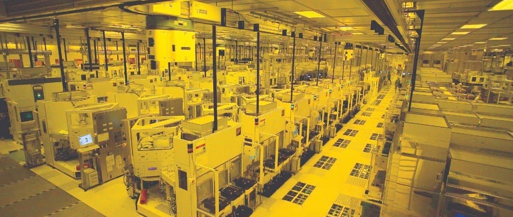
TSMC's A16 process represents a major technological advance in the industry. This 1.6 nanometer engraving fineness incorporates several decisive innovations, notably Gate-All-Around FETs transistors, Super Power Rail, and especially backside power delivery, known as Backside Power Delivery technology. These improvements will enable increased performance and significantly reduced power consumption compared to previous generations.
The production schedule for this process spans several years. TSMC plans to begin mass production of the A16 process in the second half of 2026. The first commercial products exploiting this technology, particularly NVIDIA's next-generation graphics cards dubbed Rubin Ultra and Feynman, should emerge in late 2027 or early 2028. This Feynman architecture marks a major architectural overhaul for NVIDIA's AI accelerators.
The cost of wafers engraved at 1.6 nanometers with Backside Power Delivery exceeds 30,000 dollars per unit, a significant jump compared to 2 nanometer chips, which range from 27,000 to 28,000 dollars. This cost increase is explained by the increased complexity of manufacturing equipment, reduced initial yields, and massive technological investments made by TSMC. However, the exceptional margins of the artificial intelligence market justify this substantial investment for actors in this industry.
Apple's situation deserves particular attention to understand the stakes. The California giant remains strongly demanding of production capacity at TSMC, but for now remains focused on 2 nanometer engraving. Apple has reportedly managed to monopolize over half of TSMC's production capacity on this technological node. The A20 and A20 Pro chips destined for iPhone 18, as well as future M6 processors for MacBook Air and MacBook Pro 2026, will use this technology.
The alternatives available to Apple for the future include several possible scenarios. The company could continue using 2 nanometer fineness by opting for TSMC's N2P variant, a refined version of the current process. Another possibility would be to switch directly to the 1.4 nanometer A14 process, whose technological foundations are currently being laid. Sharing A16 capacity with NVIDIA is not completely excluded, although less likely in the short term.
Financing 1.6 nanometer engraving by TSMC involves colossal investments. The Taiwan foundry would have launched a specialized factory construction project for this engraving fineness, potentially mobilizing 49 billion dollars. These facilities, equipped with latest-generation extreme ultraviolet lithography equipment, represent unprecedented technological complexity.
The crucial role of extreme ultraviolet lithography in this architecture cannot be underestimated. Dutch company ASML dominates this strategic market, its lithographic machines being indispensable for engraving sub-2 nanometer nodes. ASML's production capabilities therefore constitute a bottleneck for the entire industry, directly affecting the commissioning schedule of new processes at TSMC and its competitors.
NVIDIA does not only benefit from A16 engraving. The Taiwan foundry is also accelerating the availability of its advanced technologies on American soil, particularly in Arizona, in response to demands from Apple and NVIDIA for local production. TSMC plans to advance by nearly two years the arrival of its 2 nanometer and A16 technologies at its Phoenix plants, reflecting the strategic urgency of having production capacity on American territory.
The technological competition between TSMC and Intel also deserves mention. Intel has developed its own 18A process, equivalent to 1.8 nanometers, and even positions itself as the first to commercialize chips of this fineness in the United States. However, questions remain concerning production yields at Intel, a determining factor for long-term economic viability. TSMC retains a considerable advantage in process maturity and proven yields.
The structural impact of this change on the global technology ecosystem is profound. The emergence of artificial intelligence as the economic locomotive of the semiconductor sector redistributes alliances, investment priorities, and commercial strategies. Traditionally dominant players like Apple are discovering that technological sovereignty over new processes is no longer automatic, even for companies with considerable financial means.
Generative artificial intelligence and high-performance computing workloads now constitute the sector's core. These applications require exceptional raw performance and superior energy efficiency, criteria for which specialized processors and accelerators from NVIDIA and AMD prove particularly suitable. Apple, while developing its own Neural Engine chips, does not require the same raw computing power as artificial intelligence data centers.
The balance of power among TSMC's major customers thus reflects current macroeconomic developments. While the mobile industry stagnates slightly, massive investments in artificial intelligence infrastructure are accelerating. Data centers and computing centers represent the sector's growing demand, explaining the new commercial hierarchy established by TSMC.
Future perspectives will depend on the evolution of the artificial intelligence market and Apple's ability to innovate on mobile and mainstream computing applications. If AI remains the main engine of semiconductor demand, NVIDIA will likely retain its advantage of access to the most advanced technologies. Conversely, if the edge computing AI terminal market explodes, Apple could regain influence at TSMC through its considerable volumes.
Sources:
Clubic, "Engraving at 1.6 nm: Apple appears to have been outpaced by NVIDIA on TSMC's most advanced process"
iPhoneAddict.fr, "TSMC favors Nvidia over Apple for 1.6 nm engraving"
HardwareCooking, "NVIDIA outpaces Apple on future TSMC A16 node for its AI GPUs »
Newtechnology © 2025
Newtechnology — empowering tomorrow’s innovators, shaping a smarter future and inspiring hope for every individual.
Reframe your inbox
Subscribe to our newsletter and never miss a story.
We care about your data in our privacy policy.